RF Microwave Amplifier

This project focused on designing and constructing an RF amplifier operating at 3.0 GHz using the NPN BJT transistor AT-42086. The design process began with paper-based schematics, followed by simulation, refinement, and optimization using AWR Microwave Office. The workflow was divided into four key phases: Input Matching Network Design and Optimization, Output Matching Network Design and Optimization, RF Choke Design and Optimization, and Final Design Synthesis and Optimization. Each phase involved iterative verification and measurements to ensure optimal performance. Once individual sections were complete, the circuits were integrated, fine-tuned, and synthesized into the final amplifier design.
The matching networks were designed using distributed elements (transmission lines), specifically open-circuit shunt stubs. Key design parameters included stability, characteristic impedance, gain, input matching (source), output matching (load), DC biasing, and radial stubs. To achieve the desired gain, the transistor was biased using two independent DC power supplies configured as bias tees (incorporating RF chokes and DC blocks). Surface-mount capacitors were used to ensure the transistor was DC-isolated. The physical dimensions of the external components (transistor, capacitors, resistors) adhered to the test jig’s 2.000 × 2.750 inch specifications. The final design was exported as a high-resolution Gerber (.gbr) file for fabrication.
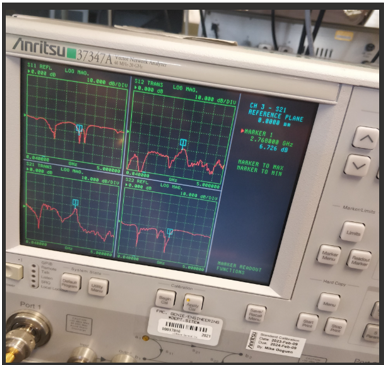
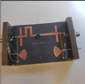
The final implementation phase involved assembling all components onto the fabricated printed circuit board (PCB) and securing it within the test jig. The process began with drilling holes in the board for fastening to the jig. DC components were soldered into place to properly bias and align the amplifier. Once the assembly was complete, the board was secured with screws. Measurements were performed using a Vector Network Analyzer (VNA) to validate the amplifier’s performance against design specifications. The fully assembled PCB fitted into the jig is shown in Figure 2.
This project successfully demonstrated the design, simulation, fabrication, and testing of an RF amplifier operating at 3.0 GHz. Using AWR Microwave Office and an iterative design process, the amplifier achieved the desired gain and stability parameters. Laboratory measurements confirmed the accuracy of the design, with the final circuit meeting all specifications. The project underscores the effectiveness of combining theoretical design principles with advanced simulation tools to produce high-performance RF amplifiers suitable for practical applications.